(Editor’s note: Dispatches Europe contributed to this post on photonics, part of our Tech Tuesday series. Dispatches covers technology because so many of our highly skilled internationals are researchers, entrepreneurs and physicists.)
For 25 years, High Tech Campus Eindhoven has been a center of technical innovation. In the past few years, it has also become an integrated photonics hub. Some in the industry go so far as to describe HTCE is a European “hotspot” for integrated photonics, with its density of organizations starting, expanding or relocating here.
As a hub, HTCE hosts not just the startups and scale-ups in the increasingly crucial integrated photonics sector but also a cross-border ecosystem of photonic chip technology organizations.
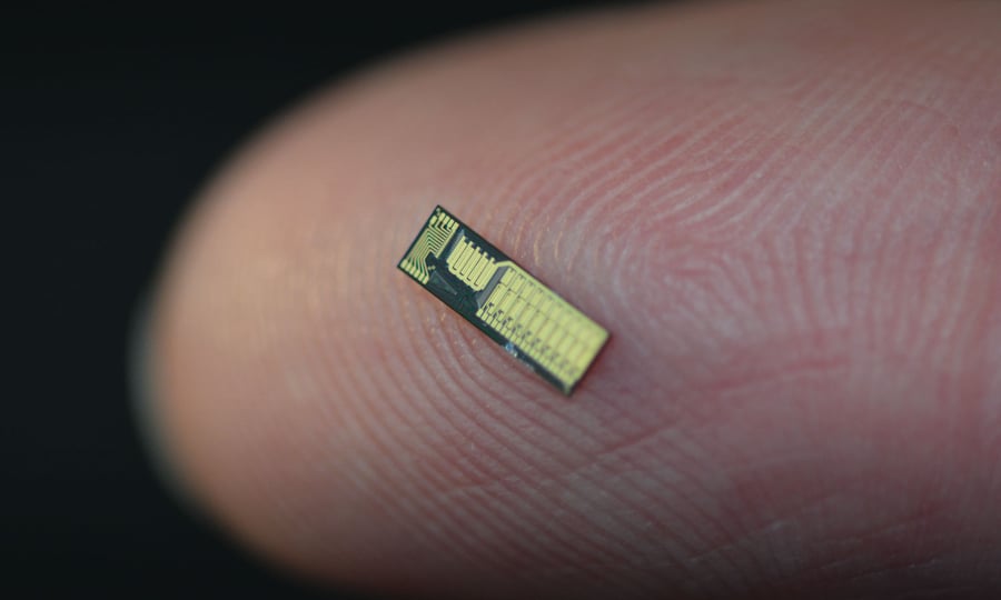
Photo copyright EFFECT Photonics
You could call PhotonDelta an “ecosystem orchestrator” for integrated photonics in the Netherlands. It’s a non-profit organization supporting an end-to-end value chain for photonic chips. Founded in 2014, PhotonDelta landed 1.1 billion euros in public and private investment capital to transform Europe into the leader of next-generation semiconductors. PhotonDelta’s headquarters is located at building HTC 31.
Integrated Photonics revolutionizing sectors
Photonic integrated circuits, or PICs, use photons (light) to transmit data. To apply a photonic chip in applications, you still need conventional chips. PICs can combine multiple photonic functions on a single chip, making photonic data transmission faster and more energy efficient.

PICs are revolutionizing multiple industry sectors, including healthcare, communications, automotive, agrifood and aerospace. To ensure Europe and the Netherlands strengthens its position as a global innovator, PhotonDelta facilitates the growth of startups, the creation of new photonic chip applications as well as the development of infrastructure and talent.
Leveraging funding from the Dutch National Growth Fund, alongside strategic investments, they catalyze the acceleration of the photonic chip industry by stimulating industrialization of PIC technology, and PIC-based application building, and forging connections with viable markets and stakeholders.

The Photonics ecosystem at High Tech Campus Eindhoven
In 2022, PhotonDelta announced it had been awarded 1.1 billion euros to fund 200 startups on the same day HighTechXL announced its partnership with PhotonDelta. As the Netherland’s only deep-tech venture builder, it made sense for HTXL to collaborate with PhotonDelta to get startups to market. If high tech is hard, deep tech is harder. Yet HighTechXL has churned out five ventures using integrated photonics sensors in five distinct industries, and PhotonDelta has provided early-stage funding for three of them.
Multiple PIC startups are forming or growing exponentially, including the Netherlands’ only Pure-play InP foundry, SMART Photonics. In 2023, EFFECT Photonics moved its operations to HTCE. The two pioneering photonics companies are neighbors at building HTC 37. SMART Photonics is a spin-off from Eindhoven University of Technology (TU/e) and Philips and was launched in 2012. It’s been based at HTCE from the early days.

EFFECT Photonics is also a spin-off from TU/e. It was founded in 2014 and moved from its Strijp-S location in late 2023 to building HTC 37. EFFECT Photonics is headquartered here and has additional facilities in the UK, the U.S. and Taiwan.
Campus resident NXP (HTC 60 and HTC 91), one of the largest chip makers in Europe, is part of a syndicate that recently invested 100 million euros in SMART Photonics to expand its manufacturing capabilities and develop new PIC technology.
While the photonics revolution is well under way, there are still technical challenges to overcome. As of early 2025, there are multiple startups focused on, or using, integrated photonics, including creating chips that can transmit data at various light wavelengths simultaneously on the same chip. Toward that end, Holst Centre in building HTC 31 is creating labs for outside companies to use for photonics research.
Here, we list all the major integrated photonics players at Campus (and nearby) by category so you can understand the dense web of a thriving ecosystem and how all the players are connected. And while most of these companies are either based at High Tech Campus or have locations here, we’ve also included companies and institutions we consider essential to the integrated photonics ecosystem but that are located outside the epicenter of HTCE.
Here’s a partial list of the photonics players on campus by listed by applicaiton. You can download the entire list here.
DATACOM/TELECOM:
EFFECT Photonics – A highly vertically integrated, independent photonic semiconductor company, EFFECT Photonics uses proprietary digital signal processing and forward error correction technology, ultra-pure light sources and integrated optical system-on-chips for communication applications.
Aircision uses proprietary laser-based free space optics to transmit data faster and over longer distances than conventional fiber.
Astrape is creating optical switches for data centers, increasing data processing speed while cutting energy consumption.
DESIGN
Synopsys creates advanced technologies for chip design, verification, IP integration, and software security and quality testing.
Bright Photonics is an independent design house for Photonic Integrated Circuits (PIC) in Silicon, III-V, SiN, Silica and Polymers. They support PIC development from application idea to prototypes and design for volume production.
FABRICATION
SMART Photonics – In 2024, the Dutch foundry has significantly scaled up its production of photonic chips by transferring its entire production capability at HTCE from 3-inch to 4-inc wafer substrates, one of the first PIC foundries to do so.
ASML is the world’s only maker of advanced UV photolithography systems for the semiconductor industry, manufacturing complex machines that are critical to the production of the next generation of integrated circuits or microchips
EQUIPMENT
PhotonFirst – PhotonFirst develops next-generation smart sensing technologies. Chip-based sensing is based on an integrated photonics chip technology, where the light is sent into the fiber with a light source and measured back directly on a photonics-based chip in the interrogator.
Etteplan – Etteplan is a publicly traded company developing technology that accelerates the transition from electronic to photonic integrated circuits (PICs), a breakthrough in cost and cycle time of the manufacturing process is needed.
Teledyne Dalsa makes MEMS (microscopic devices incorporating both electronic and moving parts) and semiconductor products at its own foundry.
LAB SPACE AND TEST FACILITIES
Holst Centre partners with imec and TNO On R&D for health technologies and flexible and wireless electronics.
TU/e, or the Technical University of Eindhoven, is one of 14 engineering schools in the Netherlands and among the highest-rated in Europe. TU/e’s Center for Integrated Photonics Eindhoven (IPI) carries out research in materials, devices, circuits and systems enabling novel applications in computing, communications and sensing.
PITC – The Photonics Integration Technology Center works with academic institutes and companies to find new, real-world applications for integrated photonics.
KNOWLEDGE, EDUCATION AND TALENT
PhotonDelta PhotonDelta/Photon Ventures fund photon startups in a deep-tech accelerator/venture builder.
Holst Centre is an independent R&D effort jointly operated by imec and TNO.
TNO is the independent, but government funded, R&D institution focusing on applied sciences. TNO’s mission is to generate innovative solutions with demonstrable impact to achieve a safe, healthy, sustainable, and digital society and boost the earning power of the Netherlands.
Imec is the Interuniversity Microelectronics Centre, an international research & development organization focusing on nanoelectronics and digital technologies
MEDICAL
VitalWear uses optical fiber sensing for non-invasive monitoring of medical conditions. Photonic measurement technology is integrated into textiles such as bed sheets, mattress covers or clothing, which enables continuous and autonomous patient monitoring with high patient comfort and with low effort for the care providers.
PACKAGING
Ettelplan has developed a flexible assembly platform for integrated photonics. The Indigo can handle a wide range of actions commonly required in the final steps of integrated-photonics manufacturing, accelerating the prototyping of photonics products
Phillips Engineering Solutions, already in conventional semiconductor and MEMS assembly, has added assembly of electronic and photonic devices from chips to boards.
SENSING
PhotonFirst uses photonic integrated chips to develop fiber-based sensing technology for measuring temperature, strain, pressure or shape.
Senergetics uses optic fibers with sensors to monitor industrial processes in extreme conditions or dangerous environments where humans can’t survive.
Spectrik uses photonic sensors to monitor farms for nitrogen pollution.
Mantispectra is developing photonic sensors using near infrared spectroscopy for a number of applications including in homes, on farms and in industry.